The Complete Guide to Semiconductors: Types, Doping & P-N Junctions Explained

Introduction

Welcome to the fascinating world of semiconductors! Whether you are reading this on a smartphone, a laptop, or a tablet, you are using millions of microscopic semiconductor devices right now. They are the foundational building blocks of modern electronics.

Here is a comprehensive guide to understanding what semiconductors are, how they are categorized, and the physics that determines how they interact with electricity and light.

What is a Semiconductor?

A semiconductor is a material with an electrical conductivity that falls somewhere between that of a conductor (like copper, which lets electricity flow freely) and an insulator (like glass, which blocks electricity).

At absolute zero temperature, a pure semiconductor acts as a perfect insulator. However, at room temperature, it gains just enough thermal energy for a small number of electrons to break free from their atomic bonds, allowing a small amount of current to flow.

The Band Theory

To understand how this works, we look at Band Theory. In solid materials, electrons exist in energy bands:

  1. Valence Band: The highest energy band that is normally filled with electrons.

  2. Conduction Band: The band above the valence band. When electrons jump into this band, they can move freely and conduct electricity.

Bandgap (Energy Gap): The energy difference between the valence and conduction bands.
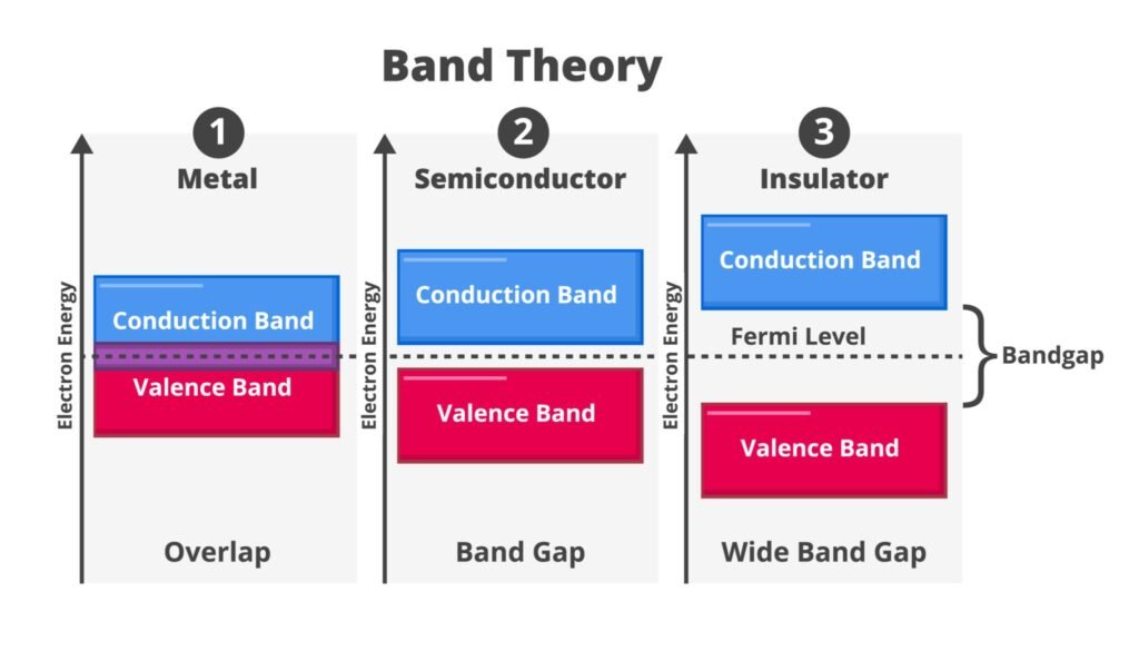
Band diagram: Semiconductor, conductor, metal

Fig :- Energy Bands: Conductor, Semiconductor, Insulator. 

  • In conductors, these bands overlap.
  • In insulators, the bandgap is huge—electrons can’t jump across.
  • In semiconductors, the bandgap is relatively small (typically between 0.1 and 3 electron-volts or eV). With a little energy push, electrons can jump the gap.

Types of Semiconductors

Semiconductors are broadly classified into two categories based on their purity: Intrinsic and Extrinsic.

1. Intrinsic Semiconductors

These are semiconductors in their purest form, with no added impurities. Silicon (Si) and Germanium (Ge) are the most common examples.

  • How it works: When an electron jumps to the conduction band, it leaves behind an empty space in the valence band called a “hole”. In an intrinsic semiconductor, the number of free electrons perfectly equals the number of holes.

  • Conductivity: Very low at room temperature.

2. Extrinsic Semiconductors

Because intrinsic semiconductors aren’t very useful for conducting current, scientists add specific impurities to them to dramatically increase their conductivity. This process is called doping. Extrinsic semiconductors are split into two types based on the dopant used:

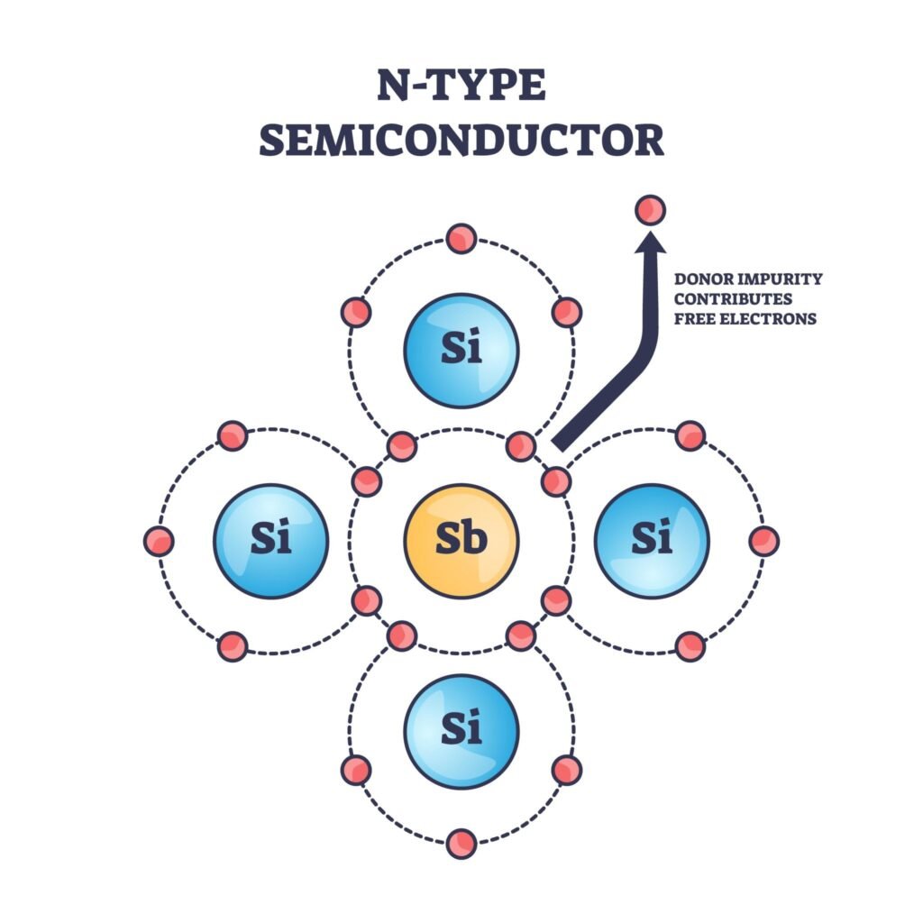
N-Type (Negative Type)

  • Doping: The semiconductor (like Silicon, which has 4 valence electrons) is doped with atoms that have five valence electrons (like Phosphorus or Arsenic).

  • Result: Four electrons form bonds, but the fifth electron is left loosely bound and easily jumps to the conduction band. The majority charge carriers are electrons.
P-Type (Positive Type)

  • Doping: The semiconductor is doped with atoms that have only three valence electrons (like Boron or Gallium).

  • Result: The dopant is missing one electron to complete the bonds, creating a “hole” (a positive charge void). Other electrons can jump into this hole, effectively moving the hole around the crystal. The majority charge carriers are holes.
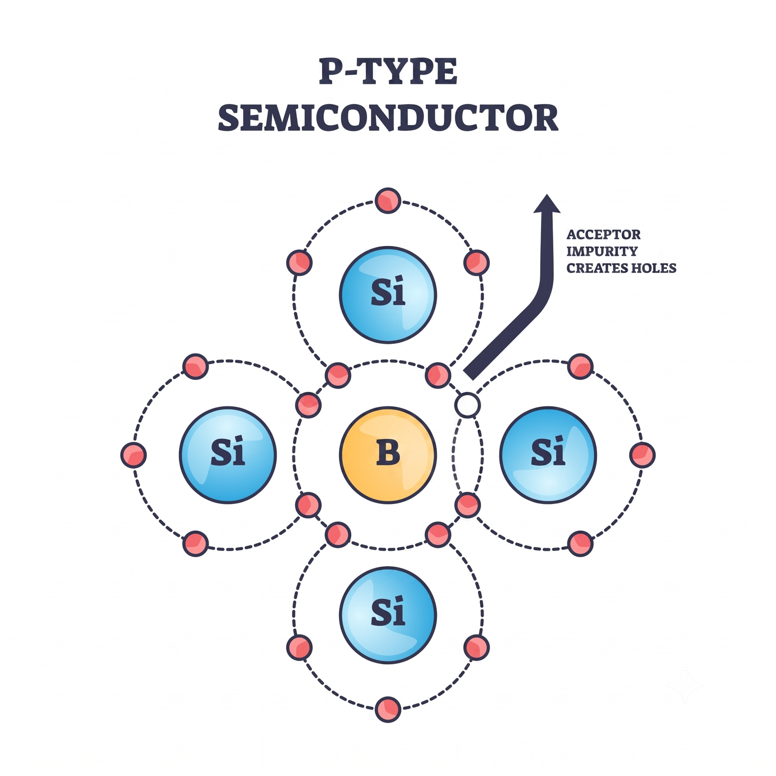
p type semiconductor

When you join a P-Type and an N-Type semiconductor together, you create a P-N Junction—the fundamental mechanism behind diodes, solar cells, and transistors.

A P-N junction is the interface formed by joining a P-type semiconductor, which has holes as majority charge carriers, with an N-type semiconductor, which has electrons as majority charge carriers.

  • P-type region: Majority carriers are holes, while electrons are minority carriers.
  • N-type region: Majority carriers are electrons, while holes are minority carriers.

When these two regions are brought into contact, they do not remain electrically isolated. Instead, the charge carriers begin to move across the junction due to a concentration difference.
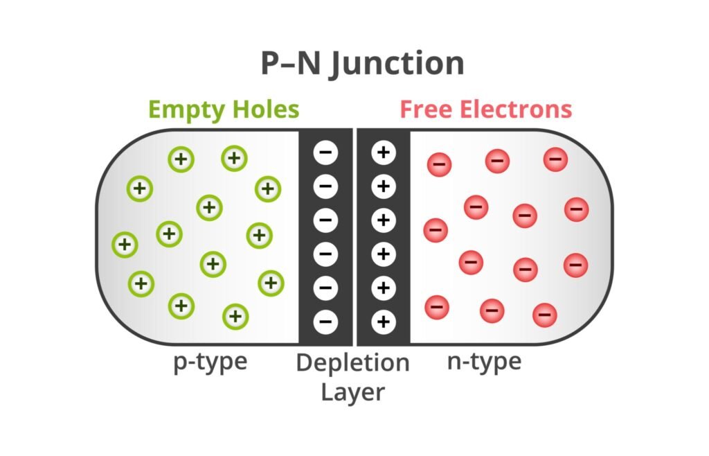
pn junction

P-N Junction showcasing Extrinsic Semiconductors.

Step 1: Diffusion of Charge Carriers

Immediately after the junction is formed:

  • Electrons move from the N-region to the P-region because the electron concentration is higher on the N-side.
  • Holes move from the P-region to the N-region because the hole concentration is higher on the P-side.

This movement of carriers due to concentration difference is called diffusion.

Step 2: Recombination

When an electron from the N-side reaches the P-side, it meets a hole.

The electron fills the hole, and both disappear as free charge carriers. This process is called electron-hole recombination.

Step 3: Formation of Immobile Ions

As electrons leave the N-region, they leave behind positively charged donor ions because the donor atoms have lost their extra electrons.

Similarly, as holes leave the P-region, negatively charged acceptor ions remain because acceptor atoms have accepted electrons.

These ions are fixed in the crystal lattice and cannot move.

Step 4: Formation of the Depletion Region

Near the junction, free electrons and holes disappear because they recombine.

As a result, this region contains almost no mobile charge carriers.

This carrier-free region is called the depletion region (also called the depletion layer or space-charge region).

Characteristics of the depletion region:

  • No free electrons
  • No free holes
  • Contains only immobile ions
  • Acts as an insulating barrier

Step 5: Formation of the Electric Field

The fixed ions in the depletion region create an internal electric field.

The electric field points from the positive donor ions (N-side) toward the negative acceptor ions (P-side).

Step 6: Formation of the Barrier Potential

The electric field creates a potential difference across the junction called the barrier potential (or built-in potential).

This barrier opposes further diffusion of electrons and holes.

Typical barrier potentials at room temperature are:

  • Silicon (Si): about 0.7 V
  • Germanium (Ge): about 0.3 V

Once this barrier is established, diffusion slows down until an equilibrium is reached.

Equilibrium Condition

At equilibrium:

  • Diffusion of carriers still tends to occur due to concentration differences.
  • The electric field in the depletion region causes a drift current in the opposite direction.

When the diffusion current equals the drift current, the net current through the junction is zero.

This is the natural equilibrium state of the P-N junction without any external voltage.

Working Under Forward Bias

In forward bias:

  • The positive terminal of the battery is connected to the P-side.
  • The negative terminal is connected to the N-side.
 
(+ Battery) ---- P | N ---- (- Battery)
 

What happens?

  1. The external voltage opposes the built-in electric field.
  2. The barrier potential decreases.
  3. The depletion region becomes thinner.
  4. Electrons easily cross from the N-side to the P-side.
  5. Holes easily cross from the P-side to the N-side.
  6. Large current flows through the junction.
 
Battery

+ -------- P | N -------- -

Barrier ↓       
Current ↑
 

A silicon diode begins to conduct significantly when the applied forward voltage is approximately 0.7 V, while a germanium diode conducts at about 0.3 V.

Working Under Reverse Bias

In reverse bias:

  • The positive terminal is connected to the N-side.
  • The negative terminal is connected to the P-side.
 
(+ Battery) ---- N | P ---- (- Battery)
What happens?
  1. The external voltage adds to the built-in electric field.
  2. The barrier potential increases.
  3. The depletion region widens.
  4. Majority carriers are pulled away from the junction.
  5. Almost no current flows.
 
Battery

+ -------- N | P -------- -

Barrier ↑

Current ≈ 0
 

Only a very small reverse saturation current, caused by minority carriers, flows until breakdown occurs at high reverse voltages.

Applications of the P-N Junction

The P-N junction is the fundamental element in many semiconductor devices:

  • Rectifier diodes: Convert AC to DC.
  • Light Emitting Diodes (LEDs): Emit light when forward biased.
  • Laser diodes: Produce coherent laser light.
  • Photodiodes: Detect light by generating current under illumination.
  • Solar cells: Convert sunlight into electrical energy.
  • Bipolar Junction Transistors (BJTs): Use two P-N junctions for amplification and switching.
  • Integrated Circuits (ICs): Contain millions to billions of P-N junctions in modern microprocessors.

Key Points to Remember

  • A P-N junction is formed by joining P-type and N-type semiconductors.
  • Electrons and holes initially diffuse across the junction due to concentration differences.
  • Recombination near the junction leaves behind immobile ions, creating the depletion region.
  • The depletion region develops an internal electric field and a barrier potential, preventing further diffusion.
  • Under forward bias, the barrier decreases, the depletion region narrows, and current flows easily.
  • Under reverse bias, the barrier increases, the depletion region widens, and only a tiny reverse saturation current flows.
  • The unique behavior of the P-N junction makes it the foundation of nearly all modern electronic and optoelectronic devices.
 

About Us

Welcome to our Physics Blog! We’re excited to take you on a journey through the fascinating world of physics, where we’ll unravel the mysteries of the universe, one topic at a time. Physics is the science that underpins everything in the natural world. It’s the key to understanding the behavior of matter, energy, and the forces that shape our reality.

Recent Posts