In the realm of analog electronics, few components hold as much prominence and enduring relevance as the IC 741 operational amplifier (op-amp). Developed by renowned electronics manufacturer Texas Instruments in the late 1960s, the IC 741 has solidified its place as one of the most widely used and versatile op-amps in history. Its enduring popularity stems from its robust performance, ease of use, and broad applicability across a myriad of electronic circuits. This article delves into the inner workings, characteristics, applications, and historical significance of the iconic IC 741 operational amplifier.
History and Development:
The genesis of the IC 741 can be traced back to the mid-20th century when the demand for high-performance amplifiers surged in various fields including telecommunications, instrumentation, and audio electronics. In response to this growing need, engineers at Texas Instruments spearheaded the development of a general-purpose operational amplifier with unparalleled performance characteristics. The result was the creation of the IC 741, which quickly gained widespread adoption due to its exceptional reliability and versatility.
Technical Overview:
At its core, the IC 741 is a monolithic integrated circuit comprising several transistors, resistors, and capacitors configured to deliver high gain and excellent operational characteristics. It operates from a dual power supply voltage typically ranging from ±5V to ±18V, although variations exist. The 741 op-amp features two inputs, namely the inverting (-) and non-inverting (+) terminals, along with a single output terminal. The differential input stage, coupled with a high-gain amplifier, enables the IC 741 to amplify small input signals with minimal distortion.
Symbol of IC 741:
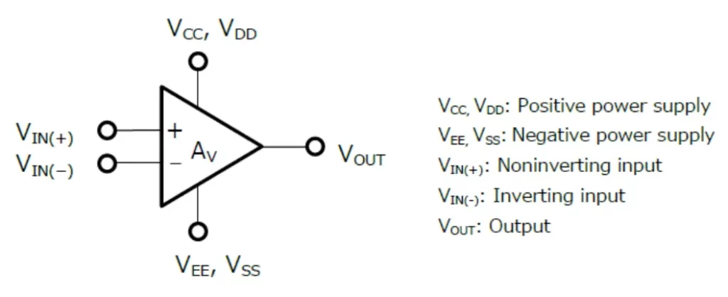
The symbol of IC 741 encapsulates its functionality succinctly. It typically comprises a triangle representing the amplifier with two input terminals, denoted as the inverting (-) and non-inverting (+) inputs, and a single output terminal. The operational amplifier’s power supply connections are indicated, usually denoted as +Vcc and -Vcc. Additionally, the ground (GND) connection is illustrated. This simplified symbol serves as a visual representation of the IC 741’s functionality, aiding in schematic designs and circuit analysis.
Pin Diagram of IC 741:
A closer look at the pin diagram of IC 741 reveals its physical configuration and connectivity:
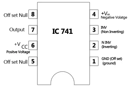
Now let’s take a look at the functions of different pins of 741 IC:
- Pin4 & Pin7 (Power Supply): Pin7 is the positive voltage supply terminal and Pin4 is the negative voltage supply terminal. The 741 IC draws in power for its operation from these pins. The voltage between these two pins can be anywhere between 5V and 18V.
- Pin6 (Output): This is the output pin of IC 741. The voltage at this pin depends on the signals at the input pins and the feedback mechanism used. If the output is said to be high, it means that voltage at the output is equal to positive supply voltage. Similarly, if the output is said to be low, it means that voltage at the output is equal to negative supply voltage.
- Pin2 & Pin3 (Input): These are input pins for the IC. Pin2 is the inverting input and Pin3 is the non-inverting input. If the voltage at Pin2 is greater than the voltage at Pin3, i.e., the voltage at inverting input is higher, the output signal stays low. Similarly, if the voltage at Pin3 is greater than the voltage at Pin2, i.e., the voltage at non-inverting input is high, the output goes high.
- Pin1 & Pin5 (Offset Null): Because of high gain provided by 741 Op-Amp, even slight differences in voltages at the inverting and non-inverting inputs, caused due to irregularities in manufacturing process or external disturbances, can influence the output. To nullify this effect, an offset voltage can be applied at pin1 and pin5, and is usually done using a potentiometer.
- Pin8 (N/C): This pin is not connected to any circuit inside 741 IC. It’s just a dummy lead used to fill the void space in standard 8 pin packages.
Specifications
The following are the basic specifications of IC 741:
- Power Supply: Requires a Minimum voltage of 5V and can withstand up to 18V
- Input Impedance: About 2 MΩ
- Output impedance: About 75 Ω
- Voltage Gain: 200,000 for low frequencies (200 V / mV)
- Maximum Output Current: 20 mA
- Recommended Output Load: Greater than 2 KΩ
- Input Offset: Ranges between 2 mV and 6 mV
- Slew Rate: 0.5V/µS (It is the rate at which an Op-Amp can detect voltage changes)
The high input impedance and very small output impedance makes IC 741 a near ideal voltage amplifier.
NOTE: The above mentioned specifications are generic and may vary from manufacturer to manufacturer. To get accurate information, please refer to the data sheet.
Key Characteristics:
The IC 741 boasts several key characteristics that contribute to its widespread utility:
- High Gain: With a typical open-loop gain exceeding 100,000, the IC 741 can amplify input signals substantially, making it suitable for applications requiring significant signal amplification.
- Wide Bandwidth: The operational bandwidth of the IC 741 extends from a few hertz to several megahertz, allowing for the amplification of signals across a broad frequency spectrum.
- Low Input Bias Current: The IC 741 exhibits minimal input bias current, ensuring that the input impedance of circuits employing this op-amp remains relatively high, thus reducing loading effects.
- High Input Impedance: With input impedance typically in the range of several megohms, the IC 741 presents minimal loading to preceding circuitry, preserving signal integrity.
- Low Offset Voltage: The offset voltage of the IC 741 is kept to a minimum, ensuring accurate amplification of small input signals without significant offset errors.
Applications:
The versatility of the IC 741 renders it indispensable in a plethora of electronic applications, including but not limited to:
- Signal Conditioning: The IC 741 is widely employed for signal conditioning tasks such as amplification, filtering, and impedance matching in sensor interfaces, instrumentation circuits, and data acquisition systems.
- Active Filters: Its high gain and bandwidth make the IC 741 well-suited for implementing active filter configurations, including low-pass, high-pass, band-pass, and band-stop filters.
- Voltage Comparator: Leveraging its differential input configuration, the IC 741 can be utilized as a voltage comparator in applications requiring precise comparison of analog voltage levels.
- Voltage Follower: In voltage buffering applications, the IC 741 serves as an efficient voltage follower, replicating the input voltage at its output with unity gain.
- Audio Amplification: Due to its low distortion and wide bandwidth, the IC 741 finds extensive use in audio amplification circuits, including microphone preamplifiers, audio mixers, and headphone amplifiers.
Conclusion:
For over half a century, the IC 741 operational amplifier has remained an indispensable tool in the arsenal of electronics engineers and hobbyists alike. Its enduring popularity can be attributed to its robust performance, ease of use, and broad applicability across a myriad of electronic circuits. As technology continues to advance, newer op-amp designs have emerged with enhanced performance characteristics. However, the IC 741’s legacy as the quintessential workhorse operational amplifier endures, serving as a testament to its timeless design and enduring relevance in the ever-evolving field of analog electronics.