Resistive Random-Access Memory (ReRAM) has emerged as a promising candidate for next-generation memory devices due to its high-speed operation, low power consumption, and potential for integration with existing semiconductor technologies. ReRAM is a type of non-volatile memory that relies on the resistance switching properties of a dielectric material (usually a metal oxide) to store data.
In this blog post, we will focus on the current-voltage (I-V) characteristics of ReRAM, particularly how the system operates between two key resistance states: Low Resistance State (LRS) and High Resistance State (HRS). Understanding the behaviour of these states is essential for grasping how ReRAM devices function in memory applications.
What is ReRAM?
ReRAM, or Resistive RAM, is a non-volatile memory technology that stores data by changing the resistance of a material in response to an applied electric field. Unlike traditional memories like DRAM or flash, ReRAM does not rely on charge storage but instead utilizes resistive switching, where the resistance of the material can be increased or decreased through the application of a voltage. This makes ReRAM both faster and more energy-efficient than conventional technologies.
Key Characteristics of ReRAM: I-V Curves
The I-V characteristics of a ReRAM device are crucial in understanding how the device operates under different conditions. When a voltage is applied across the ReRAM device, it undergoes a resistive switching process, moving between different resistance states based on the polarity and magnitude of the applied voltage.
The I-V curve of ReRAM is typically characterized by:
- Asymmetric Behaviour: The I-V curve is not symmetric due to the nature of the resistive switching process. ReRAM devices exhibit different characteristics when the voltage is swept in the positive or negative direction.
- Non-linear Behaviour: ReRAM devices display a non-linear relationship between current and voltage, particularly when transitioning between different resistance states.
- Threshold Voltage: The voltage required to initiate the switching process from one resistance state to another is called the threshold voltage. Below this voltage, the device remains in its current resistance state.
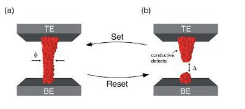
- Forming Process: Initially, a forming process is often required to set the device into a state where switching can occur. During this process, the device is subjected to a high voltage to induce a permanent conductive path, typically through the formation of conductive filaments within the material.
At the core of ReRAM functionality are two distinct resistance states: Low Resistance State (LRS) and High Resistance State (HRS). These states are a result of the resistive switching mechanism, and their characterization is key to understanding the device’s operation.
Low Resistance State (LRS)
- Description: The Low Resistance State (LRS) corresponds to the state where the ReRAM device is in its “on” state, meaning the resistance of the device is low, and it can conduct current easily. In this state, the material has been reduced to a conductive state, usually by the formation of a filamentary path through the dielectric layer (such as a metal oxide) in the device.
- Voltage Behaviour: The LRS is typically induced by applying a voltage of appropriate polarity and magnitude, which causes the dielectric material to undergo a reduction process that lowers its resistance. For instance, in a typical metal-oxide ReRAM device, the application of a negative voltage can lead to the electrochemical reduction of metal cations, creating a conducting path that lowers the overall resistance.
- Current Response: In the LRS, when a small voltage is applied, the current response is much higher due to the low resistance. The device can easily pass a higher current, which signifies the “on” or conductive state.
- Retention Characteristics: Devices in LRS have a lower resistance, meaning they can “retain” data in the form of low resistance over a longer period, as long as the device is not exposed to conditions that might disrupt the filaments or the conducting path.
High Resistance State (HRS)
- Description: The High Resistance State (HRS) corresponds to the state where the device is “off,” meaning its resistance is high, and it cannot conduct significant current. This state is typically achieved after the application of a voltage that causes the conductive filaments or conducting paths to dissolve or break apart, returning the device to a high-resistance condition.
- Voltage Behaviour: A positive voltage is generally applied to reset the device from the LRS to the HRS. This can cause oxidation of the metallic filaments or break the conductive path, increasing the resistance of the device. The threshold voltage required for this reset process is often higher than the voltage needed to set the device to the LRS.
- Current Response: In the HRS, the current response is much lower compared to the LRS due to the high resistance. A small voltage applied to the device results in very little current, essentially signaling the “off” state.
- Retention Characteristics: In the HRS, the resistance remains high, and the device retains the “off” state for a long time, preserving the data for a non-volatile period.
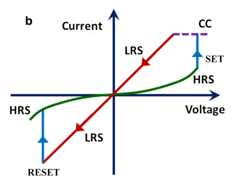
I-V Characteristics: The Switching Process Between LRS and HRS
The switching between LRS and HRS typically involves two key processes: Set and Reset.
1. Set Process (LRS):
- The device is driven into the Low Resistance State (LRS) by applying a voltage of a certain polarity and magnitude.
- For example, a negative voltage can drive oxygen vacancies or metallic filaments to form in the dielectric material, thus reducing its resistance.
2. Reset Process (HRS):
- The Reset process drives the device from LRS back to HRS by applying a voltage of opposite polarity (typically positive).
- This voltage can break or dissolve the conductive filaments that were formed during the Set process, thus increasing the resistance and returning the device to a high resistance state.
The I-V curve of a typical ReRAM device will exhibit two distinct regions: a low-resistance region (LRS) and a high-resistance region (HRS), with the device switching between these states depending on the applied voltage.
Understanding the I-V Curve of ReRAM
- Set Voltage: The voltage required to switch the device from the HRS to the LRS (the “on” state) is called the Set voltage. This voltage is typically negative and must exceed a threshold value to induce the resistive switching.
- Reset Voltage: The voltage required to switch the device from the LRS to the HRS (the “off” state) is called the Reset voltage. This voltage is usually positive and must be large enough to break the conductive filaments or disrupt the conducting path formed in the LRS.
- Asymmetric I-V Response: A typical I-V curve of ReRAM is asymmetric. The curve is steep in the negative voltage range during the Set process, while it is more gradual in the positive voltage range during the Reset process. This is due to the nature of the resistive switching, where forming the conducting path is easier than breaking it.
- Hysteresis: One of the key features of ReRAM’s I-V characteristics is hysteresis. The voltage sweeps in the positive and negative directions lead to different current responses, reflecting the non-volatile memory’s ability to store data. The hysteresis loop in the I-V curve represents the switching between LRS and HRS, showing the voltage thresholds needed to change between states.
Applications of ReRAM
ReRAM devices are particularly attractive for applications requiring high-speed, low-power, non-volatile memory. Some potential applications include:
- Non-Volatile Memory (NVM): ReRAM can replace Flash memory in certain applications due to its faster write speeds, lower power consumption, and higher endurance.
- Neuromorphic Computing: ReRAM’s analogue switching behaviour makes it suitable for mimicking synaptic connections in artificial neural networks, which is key for developing neuromorphic computing systems.
- Memory Storage: ReRAM can be used for both embedded memory storage (in mobile devices or IoT applications) and high-performance computing systems.
Conclusion
ReRAM is a highly promising memory technology with unique characteristics that make it suitable for a variety of advanced applications. The ability to switch between two resistance states—Low Resistance State (LRS) and High Resistance State (HRS)—forms the basis of ReRAM’s operation. These states are governed by the resistive switching process, which is crucial for the device’s functionality in memory storage and other applications. Understanding the I-V characteristics and the behaviour of LRS and HRS states is essential for optimizing ReRAM devices and advancing the development of next-generation memory technologies.
As research into ReRAM continues to evolve, it is expected to play a significant role in the future of computing, providing faster, more energy-efficient solutions for a wide range of applications.