Ohmic contacts are an essential component in semiconductor devices, as they facilitate the efficient flow of electrical current between the semiconductor material and external metal contacts. These contacts are designed to have a linear, low-resistance relationship between current and voltage, ensuring that they do not introduce significant resistance or alter the electrical characteristics of the device.
In this blog, we will explore the concept of Ohmic contacts, their working principles, types, and examples. Additionally, we will look at how these contacts are fabricated and their significance in real-world applications.
What is an Ohmic Contact?
An Ohmic contact is a type of electrical junction where the current-voltage relationship follows Ohm’s Law, which states that:
V = I R
Where:
- V is the voltage across the contact,
- I is the current flowing through the contact,
- R is the resistance of the contact.
In simple terms, Ohmic contacts allow current to flow freely in both directions without introducing any significant resistance or creating a barrier to current flow. This behaviour is crucial in ensuring the functionality of semiconductor devices, such as diodes, transistors, solar cells, and LEDs.
For a contact to be considered Ohmic, it must have the following characteristics:
- Low Resistance: The contact must exhibit a minimal and stable resistance across a wide range of applied voltages.
- Linear Current-Voltage (I-V) Characteristics: The relationship between current and voltage should be linear, meaning the I-V curve should resemble a straight line.
- No Rectification: Unlike Schottky contacts, Ohmic contacts do not create any rectifying behaviour (which means no forward bias behaviour in a diode). In other words, the contact should allow current to flow easily in both directions.
Key Factors Influencing Ohmic Contacts:
- Material Selection: The metal used in the contact must form a proper chemical bond with the semiconductor material.
- Semiconductor Doping: The level of doping in the semiconductor material impacts the barrier height and the ability to create a low-resistance path.
- Temperature: The temperature affects the carrier mobility and the contact resistance, so Ohmic contacts should be stable across operating temperatures.
Types of Ohmic Contacts
1. Ohmic Contact in Metal-Semiconductor Junctions
When a metal is brought into contact with a semiconductor, an energy barrier forms at the interface, which could either allow or block the current. If this barrier is small enough, the metal-semiconductor junction can behave as an Ohmic contact. The barrier height is influenced by the semiconductor’s doping level and the metal’s work function.
- N-type Semiconductor (n-type): If a metal has a lower work function than the semiconductor, it will inject electrons into the semiconductor, reducing the barrier and making the contact Ohmic.
- P-type Semiconductor (p-type): If the metal has a higher work function, it will create a barrier that can reduce the current flow, but if this barrier is small, it still qualifies as an Ohmic contact.
Example: Gold (Au) on N-type Silicon (Si)
Gold (Au) is often used as an Ohmic contact for N-type silicon. The electron affinity and the metal’s work function align in such a way that no significant Schottky barrier forms, and the contact remains linear under voltage biasing.
2. Forming Ohmic Contacts Using Alloying
Sometimes metals are alloyed with semiconductor materials to improve the performance of the contact. By controlling the composition and temperature during alloying, the metal-semiconductor interaction can be optimized to reduce the contact resistance.
Example: Aluminium (Al) on Silicon (Si)
Aluminium is a common material used to form Ohmic contacts to N-type and P-type silicon. In a typical process, aluminium is evaporated onto the surface of silicon and then annealed (heated) to form an alloy with the silicon at the junction. The alloyed region forms a low-resistance Ohmic contact.
3. Ohmic Contacts in Vertical and Lateral Devices
In vertical devices like power transistors, the contact is applied to the side of the device to connect with the semiconductor material. For lateral devices, such as integrated circuits (ICs), the contact is applied to the top surface. The properties of Ohmic contacts are equally essential in both cases, although the fabrication methods and material choices may vary.
Fabrication of Ohmic Contacts
Creating an efficient Ohmic contact involves several steps, primarily focusing on choosing appropriate materials and ensuring proper fabrication techniques to minimize contact resistance.
Steps in Fabricating Ohmic Contacts:
- Surface Cleaning: The semiconductor surface must be thoroughly cleaned to remove any oxide layer or contaminants that could affect the contact quality. This is typically done using chemical etching or plasma cleaning.
- Metal Deposition: Metals like gold, silver, or aluminium are deposited onto the semiconductor surface using techniques such as evaporation, sputtering, or electroplating. The metal forms the initial contact layer.
- Annealing: After deposition, the contact is often annealed (heated) to allow the metal atoms to diffuse into the semiconductor and form an alloy at the interface. This step is crucial for minimizing the contact resistance and ensuring good electrical conductivity.
- Patterning: In devices like ICs, photolithography is used to define specific areas where the metal contacts should be formed. This process allows precise control over the contact geometry.
- Testing: After the Ohmic contacts are fabricated, they are tested using I-V measurements to ensure that they exhibit a linear current-voltage relationship, confirming that the contact is indeed Ohmic.
Example Applications of Ohmic Contacts
1. Transistors (BJT, MOSFET)
In bipolar junction transistors (BJTs) and field-effect transistors (FETs), Ohmic contacts are used to connect the semiconductor regions (emitter, collector, source, and drain) to external electrical circuits. Without efficient Ohmic contacts, these devices would suffer from high contact resistance, which would reduce their performance.
2. Solar Cells
In solar cells, the electrodes that collect the generated current from the semiconductor material need to be Ohmic. These electrodes must have low resistance to ensure maximum efficiency in converting sunlight into electrical power.
3. LEDs (Light Emitting Diodes)
In LEDs, both the anode and cathode contacts must form Ohmic contacts with the semiconductor material (such as GaN or InGaN) to allow current to flow efficiently through the device. A high-quality Ohmic contact is essential for the efficient operation of LEDs.
Diagram of an Ohmic Contact
Below is a simple schematic diagram showing the formation of an Ohmic contact between a metal and a semiconductor:
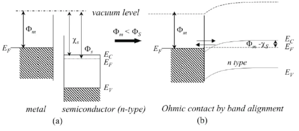
In this diagram:
- The metal (top layer) is in contact with the N-type semiconductor (bottom layer).
- The metal forms an Ohmic contact because the energy barrier between the metal and semiconductor is low enough that current can flow easily in both directions.
- No rectifying behaviour is observed; the I-V characteristic is linear.
Challenges in Ohmic Contacts
1. High Contact Resistance
One of the challenges in fabricating Ohmic contacts is minimizing the contact resistance. High contact resistance can affect device performance, especially in low-power applications, where it can cause power loss and signal distortion.
2. Material Compatibility
The choice of materials is critical. Metals and semiconductors must be compatible, and their properties must align to create low-resistance contacts. Mismatched materials could result in high barriers, leading to non-Ohmic behaviour.
3. Temperature Sensitivity
Some Ohmic contacts may degrade at high temperatures, leading to increased resistance. This is particularly important for power electronics, where devices operate under high current and temperature conditions.
Conclusion
Ohmic contacts are integral to the functionality of many electronic and optoelectronic devices, ensuring that current flows efficiently between metal electrodes and semiconductor materials. Understanding the principles behind Ohmic contacts, their fabrication, and their role in various applications helps in designing better and more efficient devices.
By ensuring that the contact is low-resistance and linear in behaviour, engineers can optimize the performance of semiconductor-based devices such as transistors, solar cells, LEDs, and more. The continuous advancement in material science and fabrication techniques is key to overcoming challenges and improving the quality of Ohmic contacts in modern electronics.