Semiconductors are the backbone of modern electronics, powering everything from smartphones to computers and beyond. At the heart of their functionality lies a crucial characteristic known as the bandgap. Bandgap determines a semiconductor’s ability to conduct electricity and influences its optical properties. Understanding the various types of bandgaps is fundamental to harnessing the full potential of semiconductor materials. In this article, we delve into the intricacies of different bandgap types and their significance in semiconductor physics and technology.
Direct Bandgap:

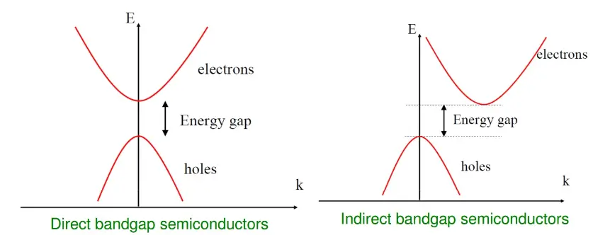
Direct bandgap semiconductors are characterized by electron transitions between the conduction band and the valence band that occur with minimal momentum change. In these materials, the energy difference between the conduction band minimum (CBM) and the valence band maximum (VBM) is relatively small, facilitating efficient light emission and absorption processes. This property makes direct bandgap semiconductors ideal for optoelectronic applications such as LEDs, lasers, and photodetectors. Prominent examples include gallium nitride (GaN) and indium phosphide (InP).
Indirect Bandgap:
Indirect bandgap semiconductors exhibit electron transitions between the conduction and valence bands that involve a significant change in momentum. As a result, these materials typically have lower absorption and emission rates compared to direct bandgap semiconductors. Silicon (Si) is a classic example of an indirect bandgap semiconductor. While less suitable for light-emitting devices, indirect bandgap materials find extensive use in electronics, particularly in integrated circuits and solar cells.
Wide Bandgap:
Wide bandgap semiconductors have bandgaps significantly larger than those of conventional materials like silicon. This characteristic enables them to operate at higher temperatures and voltages while maintaining stability and efficiency. Wide bandgap semiconductors are crucial for high-power and high-frequency applications, including power electronics, RF amplifiers, and electric vehicles. Silicon carbide (SiC) and gallium nitride (GaN) are leading contenders in this category, offering superior performance in demanding environments.
Tunable Bandgap:
Tunable bandgap semiconductors possess the unique ability to adjust their bandgap energies through external stimuli such as strain, electric field, or doping. This versatility allows for tailored electronic and optical properties, opening avenues for novel device designs and applications. Quantum dots, nanowires, and perovskite materials are examples of structures where bandgap tuning is actively explored, promising advancements in areas like flexible electronics, sensors, and quantum computing.
Gradient Bandgap:
Gradient bandgap semiconductors feature a gradual variation in bandgap energy across the material’s thickness or composition. This gradual transition can enhance charge carrier transport, reduce recombination losses, and improve device performance. Gradient bandgap structures find use in various applications, including heterojunctions, tandem solar cells, and photonic devices, where precise control over electronic properties is paramount.
Conclusion:
Bandgap engineering lies at the heart of semiconductor technology, enabling the design and optimisation of devices for diverse applications. Understanding the different types of bandgaps – from direct and indirect to wide, tunable, and gradient – provides insights into the capabilities and limitations of semiconductor materials. As research continues to push the boundaries of material science and device engineering, harnessing the full potential of bandgap engineering promises innovations that will shape the future of electronics and beyond.


