Thin films are fundamental components in many cutting-edge technologies, from microelectronics and solar cells to sensors, optics, and coatings. The formation of thin films requires precise material synthesis methods to achieve the desired thickness, composition, and properties. In this blog, we will explore various material synthesis processes used for thin film formation, their advantages, disadvantages, and key applications.
What Are Thin Films?
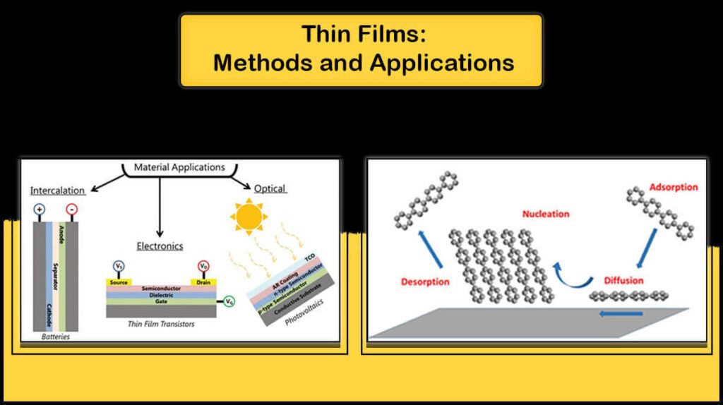
Thin films are materials with a thickness ranging from a few nanometers to several micrometers. They are applied to substrates to modify the properties of the surface or to create entirely new functionalities. Thin films are essential in areas like semiconductors, optics, energy storage devices, and protective coatings due to their unique physical and chemical properties.
Key Synthesis Processes for Thin Film Formation
1. Physical Vapor Deposition (PVD)
Physical Vapor Deposition (PVD) is one of the most widely used thin film deposition techniques. It involves the condensation of a vaporized material onto a substrate in a vacuum environment. The material is usually heated until it evaporates or sublimates, and the vapor is transported through the vacuum to condense onto the cooler substrate, forming a thin film.
Types of PVD Techniques:
- Evaporation Deposition: In this technique, the material is heated in a vacuum chamber until it evaporates and condenses on the substrate. Evaporation is often used for metal films like gold, silver, and aluminum.
- Sputtering: A target material is bombarded with high-energy particles (usually ions) causing atoms or molecules to be ejected and deposited onto the substrate. Sputtering is widely used for metal, dielectric, and semiconductor thin films.
Advantages:
- High purity and density of films.
- Precise control over film thickness.
- Versatility in material types (metals, ceramics, polymers).
Disadvantages:
- Requires high vacuum conditions, making it more expensive.
- Line-of-sight deposition can lead to non-uniform film thickness in complex geometries.
Applications:
- Semiconductor devices (e.g., transistors, memory devices).
- Optical coatings (e.g., anti-reflective coatings, mirrors).
- Thin-film solar cells.
2. Chemical Vapor Deposition (CVD)
Chemical Vapor Deposition (CVD) is a process where reactive gases are introduced into a reaction chamber, and a chemical reaction occurs at the surface of the substrate, resulting in the deposition of a solid thin film. This process is highly versatile and can produce films with varying compositions and structures.
Types of CVD Techniques:
- Low Pressure CVD (LPCVD): Conducted at low pressures, LPCVD enables better film uniformity and high-quality films with fewer defects.
- Atmospheric Pressure CVD (APCVD): This technique operates at atmospheric pressure, which makes it simpler and cheaper, but often results in less uniform films.
- Metal-Organic CVD (MOCVD): Used for depositing compound semiconductor materials, MOCVD uses metal-organic precursors.
Advantages:
- High film quality with excellent uniformity.
- Can deposit a wide range of materials, including metals, semiconductors, and insulators.
- Suitable for complex substrates.
Disadvantages:
- High temperature requirements.
- Potential toxicity and safety concerns from precursors.
Applications:
- Microelectronics (e.g., gate oxides, high-k dielectrics).
- Photovoltaic cells (e.g., CIGS solar cells).
- Wear-resistant coatings.
3. Sol-Gel Deposition
The sol-gel process involves transitioning a solution (sol) of metal alkoxides or salts into a gel state, which then forms a thin film upon deposition. This process is particularly useful for producing oxide thin films, like silica, titania, and zirconia.
Process:
- The precursor material is dissolved in a solvent and then chemically processed to form a sol.
- The sol is applied to the substrate by techniques like spin coating, dip coating, or spraying.
- After deposition, the film is dried, and heat-treated to remove residual solvents and achieve the final film properties.
Advantages:
- Low-cost process that can be done at relatively low temperatures.
- Can create films with good uniformity over large areas.
- Flexibility in material selection (oxide films, ceramics, and composites).
Disadvantages:
- The need for post-deposition heat treatment to remove organic solvents.
- Films can have lower mechanical strength compared to other deposition techniques.
Applications:
- Protective coatings for electronics.
- Photovoltaic materials.
- Catalytic and sensor coatings.
4. Atomic Layer Deposition (ALD)
Atomic Layer Deposition (ALD) is a precise deposition method used to create ultra-thin films. It involves alternating exposures of the substrate to two different chemical precursors, each reacting with the surface in a self-limiting manner. This ensures atomic-level control of film growth.
Process:
- The substrate is exposed to a precursor gas.
- The reaction is allowed to complete, and then the excess precursor is purged.
- A second precursor is introduced, and the process repeats layer by layer.
Advantages:
- Atomic-level control over film thickness and composition.
- Excellent uniformity, even on complex or 3D substrates.
- High precision for very thin layers (from a few Ångströms to tens of nanometers).
Disadvantages:
- Slow deposition rates, making it less suitable for large-scale production.
- Requires specialized equipment.
Applications:
- High-performance semiconductor devices (e.g., transistors, capacitors).
- Protective coatings.
- Supercapacitors and batteries.
5. Molecular Beam Epitaxy (MBE)
Molecular Beam Epitaxy (MBE) is a highly controlled method for growing single-crystal thin films by directing molecular or atomic beams onto a substrate in a vacuum. The material is typically deposited in ultra-thin layers, creating high-quality crystalline films.
Process:
- The substrate is heated in a vacuum chamber.
- Molecular beams of the desired material are directed at the substrate, where they condense and form a thin crystalline layer.
Advantages:
- High-quality epitaxial growth with excellent crystal structure.
- Precise control over composition, thickness, and doping.
- Ideal for complex semiconductor and heterostructure fabrication.
Disadvantages:
- Slow deposition rates.
- Requires ultra-high vacuum conditions and expensive equipment.
Applications:
- Semiconductor devices (e.g., quantum wells, LED structures).
- Optoelectronics.
- Nanoscale materials.
6. Laser Ablation (Pulsed Laser Deposition – PLD)
Pulsed Laser Deposition (PLD) is a process where a high-energy laser pulse is focused onto a target material, causing material to be ejected in the form of vapor and ions. This material then condenses onto the substrate, forming a thin film.
Advantages:
- Ability to deposit a wide range of materials, including complex compounds.
- High deposition rates compared to other methods.
- Can create high-quality films with good stoichiometry.
Disadvantages:
- Requires high vacuum conditions and sophisticated laser equipment.
- Limited scalability for large-area deposition.
Applications:
- Superconducting films.
- Thin films for optical and electronic devices.
- Hard coatings and thin-film nanostructures.
Conclusion
Thin film deposition is a critical process in the development of a wide range of technologies, from semiconductors to solar cells and optical devices. The choice of material synthesis process depends on several factors, including the type of material being deposited, the desired film properties, and the application’s requirements for scalability, cost, and quality.
Whether using Physical Vapor Deposition (PVD), Chemical Vapor Deposition (CVD), Sol-Gel methods, Atomic Layer Deposition (ALD), Molecular Beam Epitaxy (MBE), or Pulsed Laser Deposition (PLD), each technique offers unique advantages and limitations. Understanding these processes is crucial for advancing technology and developing next-generation devices with enhanced performance and new functionalities.